
Page 40 - Computer_Science_F5
P. 40
sequential logic circuits shall not be discussed in this book. The combinational and
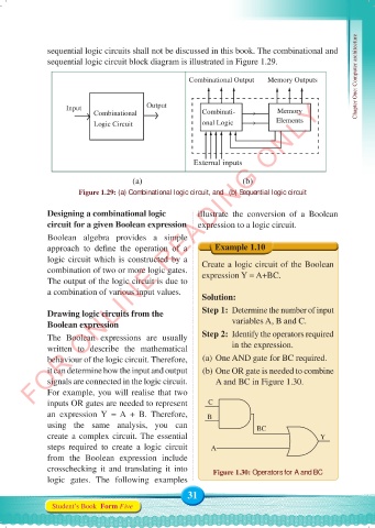
sequential logic circuit block diagram is illustrated in Figure 1.29.
Combinational Output Memory Outputs Chapter One: Computer architecture
FOR ONLINE READING ONLY
Input Output
Combinational Combinati- Memory
Logic Circuit onal Logic Elements
External inputs
(a) (b)
Figure 1.29: (a) Combinational logic circuit, and (b) Sequential logic circuit
Designing a combinational logic illustrate the conversion of a Boolean
circuit for a given Boolean expression expression to a logic circuit.
Boolean algebra provides a simple
approach to define the operation of a Example 1.10
logic circuit which is constructed by a Create a logic circuit of the Boolean
combination of two or more logic gates. expression Y = A+BC.
The output of the logic circuit is due to
a combination of various input values.
Solution:
Drawing logic circuits from the Step 1: Determine the number of input
Boolean expression variables A, B and C.
The Boolean expressions are usually Step 2: Identify the operators required
written to describe the mathematical in the expression.
behaviour of the logic circuit. Therefore, (a) One AND gate for BC required.
it can determine how the input and output (b) One OR gate is needed to combine
signals are connected in the logic circuit. A and BC in Figure 1.30.
For example, you will realise that two
inputs OR gates are needed to represent C
an expression Y = A + B. Therefore, B
using the same analysis, you can BC
create a complex circuit. The essential Y
steps required to create a logic circuit A
from the Boolean expression include
crosschecking it and translating it into Figure 1.30: Operators for A and BC
logic gates. The following examples
31
Student’s Book Form Five
Computer Science Form 5.indd 31 23/07/2024 12:32